Researchers tune the properties of a known semiconducting material so that it behaves like a metal, with some superconducting behavior, for more efficient electronic devices.
Semiconductor materials have revolutionized the electronic industry, and are currently used extensively in technologies ranging from sensors to TVs to mobile devices. The earliest transistors were built using germanium as the semiconducting material, however, silicon became the preferred material beginning in the early 1960s due to its greater abundance and low cost.

The electronic properties of semiconducting materials can be easily tuned by incorporating even minuscule amounts of other elements, and a wide range of materials of varying capabilities have been reported to date.
Now, researchers from Swansea University and the University of Rostock have demonstrated that they can create semiconducting materials that behave like metals and even superconductors by modifying their surface crystal structure. According to the reseachers, their discovery opens the door to enhancing the efficiency of electronic devices.
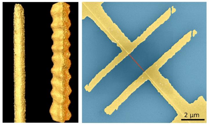
In their study, recently published in Advanced Functional Materials, they describe a method to change the electronic properties of colloidal lead sulfide (PbS) nanowires by faceting the crystal in a distinct way. While various forms of PbS nanostructures are semiconducting, when the crystal was cut through what is called the {111} facet, the resulting wires became zigzag shaped and contained a single element Pb face, which had metallic character.
Through various theoretical and in-lab experiments, the researchers were able to show that the new PbS nanowires were able to carry higher currents than their semiconductor counterparts, that their transistor behavior was suppressed, that they do not respond to illumination (which is typical of semiconductors), and that they showed inverse temperature dependency typical for metals.
“After we discovered that we can synthesize lead sulfide nanowires with different facets, which makes them look like straight or zigzag wires, we thought that this must have interesting consequences for their electronic properties,” said Dr. Mehdi Ramin, one of the study’s authors, in a press release. “But these two behaviors were quite a surprise to us. Thus, we started to investigate the consequences of the shape in more detail.”
Ramin and his co-workers were also able to show that at low temperatures their nanowires behave like a superconductor — a material (usually an element or metal alloy) that when cooled below a certain threshold temperature loses all electrical resistance. 2D superconductors have been difficult to realize, but the Pb‐rich surface of these crystals includes one monolayer of Pb atoms. “We assume that the semiconducting body of zigzag wires could also play a crucial role to support the 2D superconducting surface, similar to the previous observations of superconductivity through low‐dimensional materials supported by semiconducting substrates,” stated the authors in their study.
“This behavior is astonishing and certainly needs to be further studied in much more detail,” said Professor Christian Klinke of Swansea University and Rostock University, and the project’s lead. “But it already gives new exciting insights into how the same material can possess different fundamental physical properties depending on its structure and what might be possible in the future.
One potential application is lossless energy transport, which means that no energy is wasted. Through further optimization and transfer of the principle to other materials, significant advances can be made, which might lead to new efficient electronic devices. The results presented in the article are merely a first step in what will surely be a long and fruitful journey towards new thrilling chemistry and physics of materials.”
These results represent a new exciting platform to further optimize other colloidal materials and to predictably tune their properties according to the target application.
Reference: M. M. Ramin Moayed, et al. ‘Function Follows Form: From Semiconducting to Metallic toward Superconducting PbS Nanowires by Faceting the Crystal‘, Advanced Functional Materials (2020). DOI: 10.1002/adfm.201910503
Quotes adapted from press release provided by Swansea University

