Near-infrared sensors and displays developed based on the maximized efficiency of optical wavelength conversion.
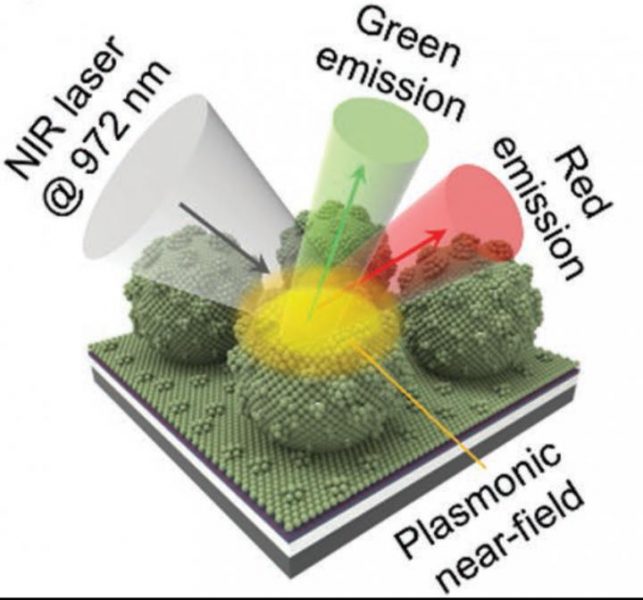
Researchers from the Korea Institute of Science and Technology (KIST) have developed a means of better visualizing infrared radiation by “translating” it into the visible spectrum using a multi-functional luminescent film. The material contains a new, microscale surface structure that can visualize near-infrared light through wavelength conversion, a process in which light is converted into longer or shorter wavelengths depending on the material being used. Their findings were recently published in Advanced Functional Materials.

“The conversion of invisible infrared or ultraviolet light into visible light allows us to intuitively see the data contained in the light, and thus enables the use of infrared or ultraviolet light for displays or imaging devices,” said the study’s authors in a press release published by KIST. “Quantum dots, recently used for high-definition TVs, can be seen as a type of wavelength conversion technology that converts ultraviolet light into visible light in displays.”
Converting high-energy ultraviolet light into visible light is relatively easy and occurs with high efficiency, according to the authors. though this is more difficult with low-energy infrared light, occurring at approximately 0.01% to 0.001% of the efficiency of converting quantum dots to visible light. “This was a major stumbling block in making near-infrared-to-visible light conversion more realistic for wider applications in various fields in the form of sensors, displays, and imaging devices.”
“Existing infrared sensors can only collect one type of data, but this technology can be used to collect various types of data all at once and visualize them,” said Dr. Kwon Seok-joon from KIST, who led the study. “Since this technology has various advantages in processing, such as foldability, washability, and transferability into other films, its application can be extended throughout various fields, and it can be used for foldable devices, wearable sensors, and flexible wavelength conversion imaging devices.”
The new material is made of a square lattice array of oxidized silicon microbeads decorated with nanoparticles that convert the longer, lower energyinfrared waves to higher energy visible light. The team was able to maximize both the absorption of near-infrared light and the luminescence of visible light with their surface microscale lattice, thus increasing the efficiency of near-infrared-to-visible light conversion by nearly 1,000 times.
The lattice was also found to be easily transferable to a transparent film, which is flexible, foldable, and even washable with the light intensity maintained after wavelength conversion.
“The expanded multi‐functionality of the plasmonic platform and its ultra‐strong [conversion] will provide substantial benefits and promote a wider range of practical applications in wearable near-infrared‐to‐visible displays and attachable/detachable sensors,” stated the authors in their study.
Reference: I.‐H. Ahn, et al. ‘A Multi‐Functional Highly Efficient Upconversion Luminescent Film with an Array of Dielectric Microbeads Decorated with Metal Nanoparticles‘, Advanced Functional Materials (2020). DOI: 10.1002/adfm.201909445

